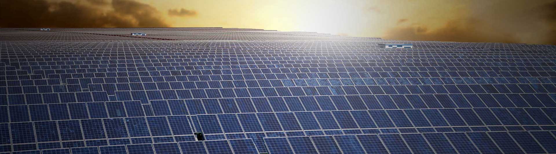
Process Technology Route
In the past two years, monocrystalline silicon has developed rapidly. Relevant data shows that the cost gap between monocrystalline silicon wafers and polycrystalline silicon wafers is rapidly narrowing, while the advantages of monocrystalline conversion efficiency are continuously expanding. The edge effect of polycrystalline cells begins to appear after reaching the conversion efficiency of 18-19%, and the growth is slow, while the conversion efficiency of P-type monocrystalline has reached about 23%, and the conversion efficiency of N-type monocrystalline has reached 23.5%-25%. The 2022 edition of the International Technology Roadmap for Photovoltaics (ITRPV) predicts that the market share of monocrystalline silicon will continue to increase, the market share of polycrystalline silicon(p-type casted) will gradually decrease, and, with the increasing investment in downstream N-type monocrystalline production, the demand for N-type monocrystalline ingots will continue to increase, and the next 10 years will be a period of rapid growth for the N-type monocrystalline market.
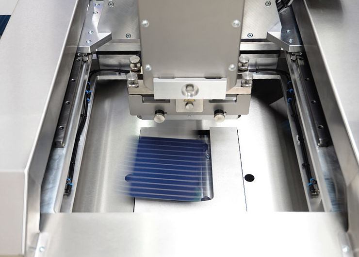
Revolutionary printing technology
There are two main processes for the production of monocrystalline silicon, namely Czochralski monocrystalline(CZ) silicon and Floating zone(FZ) monocrystalline silicon. The Czochralski monocrystalline silicon process accounts for more than 90% of the total production capacity, and the production process technology is mature and safe.
As a new cutting technology, diamond wire cutting has the advantages of thinning cutting, reducing kerf loss, reducing silicon material loss, improving processing efficiency, increasing wafer yield, reducing sewage and COD emissions, etc., which can greatly reduce the cost of silicon wafer production enterprises, improve the quality of silicon wafers. Since 2015, due to the introduction of diamond wire cutting technology in the silicon wafer section, the cost of monocrystalline silicon wafers has dropped rapidly. At present, multi-wire diamond wire cutting monocrystalline silicon wafers have reached 100% of the market share.
Monocrystalline PERC solar cells (passivated emitter rear contact solar cells) are based on conventional cells by adding two processes of passivation of Al2O3 film on the back of the cell and laser contact opening, and the absolute conversion efficiency can be improved by 1.2- 1.5%, and the average conversion efficiency reaches 22.5-23%. This project adopts the process route of growing passivation layer by tube PECVD to prepare PERC cell. The process technology is mature with high market share.
PV Cell Solution
Our solution can be matched with large size,half-cut cell,MBB,bifacial and double glass cutting-edge technology routes.
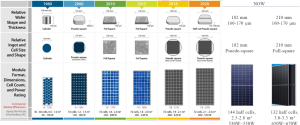
Our solution will adopt the optimal 182mm size, compatible with 210mm process route. We will adopt the optimal solution with a standard configuration of 10BB and compatible with the 5-15 BB process route.
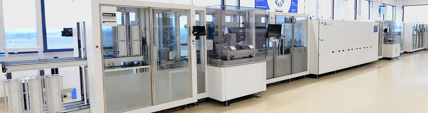
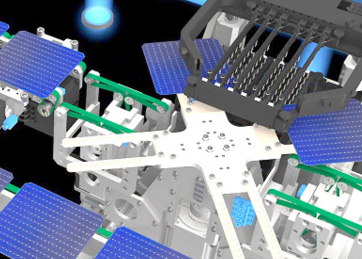
Industry 4.0 meets clever machine design
At SIEMER, we have attached great importance to optimum accessibility to all systems. We also use industry 4.0 technology to support the operator.
- Refill paste and change sieve in ergonomic position and in close proximity. Free access to all controls.
- The intuitive SIMPLEX HMI, makes machine operation faster, safer and reduces training effort.
- The operator is informed at every point about the status of the entire line and can control his cluster systems via a central touch screen HMI. Handling systems can also be operated mobile via tablet.
- Loaders and unloaders are AIV (AGV) ready, i.e. they can be connected to autonomous transport robots.
Technology for future
Our made in Germany Technology in the best sense of the word. We have customers who have been using our PV solar solutions for more than 5 years. This is only possible because we have always attached importance to scalability and upgradeability. With the SIEMER solution we go one step further. All upgrades (except the addition of a fourth pressure step) are merely retrofits in the machines:
- Upgrade to double print
- Upgrade to new cell formats: Wafer size m1-m4 and larger on request
- Upgrade to new cell technologies: PERC, SE, BSF, HJT, Back-Contact-Cells, p-Type, n-Type, Mono, Multi
We will be happy to advise you
Do you have any questions? Find your local contact with our Contact Finder.