
Complete n-type cell lines engineered for the technology route you commit to, TOPCon, HJT or back contact.
These are not variants of one line. The technology route sets the thermal budget, the cleanliness class, the deposition toolset and the metallisation method, and it constrains how the finished cells can be interconnected into modules. Choosing it is the first engineering decision, not a later configuration option.
| Criterion | TOPCon | HJT | BC |
|---|---|---|---|
| Cell efficiency | 25.0 – 26.5% | 25.0 – 26.5% | 26.0 – 27.5% |
| Process temperature | High (> 800 °C steps) | Low (< 200 °C throughout) | Depends on base route |
| Process steps | More, around 12–14 | Fewer, around 6–8 | Most, patterning added |
| Bifaciality | ≈ 0.80 – 0.85 | ≈ 0.90 – 0.95 | Varies by design |
| Temperature coefficient | Good | Best in class | Good to very good |
| Cleanliness demand | Standard cell-line class | Very high, surface critical | High |
| Silver consumption | Moderate | Higher (low-temp paste) or Cu plating | Route dependent |
| Indium / TCO need | None | Yes, ITO or IWO sputtering | Route dependent |
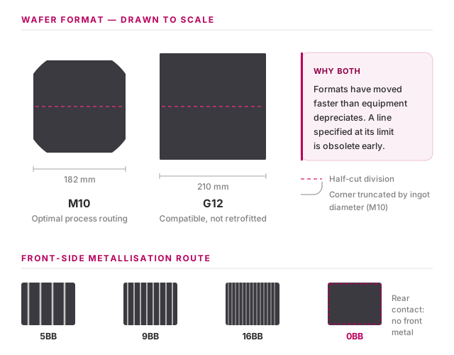
| Module interconnection | Conventional soldering | Low-temperature methods only | Specialised, often 0BB |
| Relative line capex | Lowest of the three | Higher, PECVD and PVD heavy | Highest, precision patterning |
| Best fit | Capacity scale-up with contained risk | Hot climates, high energy yield, bifacial | Premium efficiency and aesthetics |
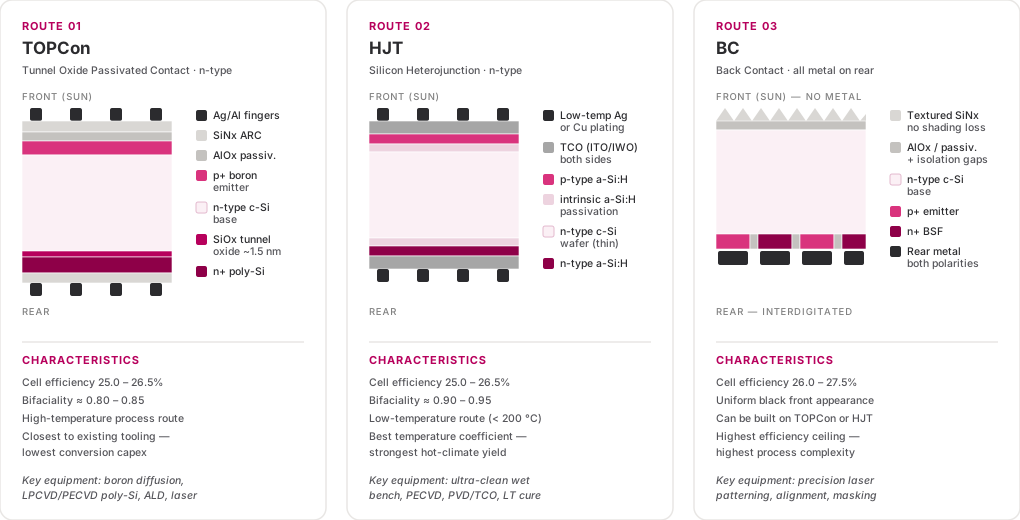
Tunnel oxide passivated contact. A thin tunnel oxide plus doped polysilicon layer on the rear delivers excellent surface passivation while still allowing carrier extraction, reached through a largely conventional high-temperature process route.
Tunnel oxide thickness uniformity and the completeness of wrap-around poly removal drive both efficiency and yield. Both are equipment and process-control problems rather than material problems, which is why they belong in the line engineering specification.
Silicon heterojunction. Thin intrinsic and doped amorphous silicon films passivate the crystalline wafer on both sides, with transparent conductive oxide carrying current laterally to the metal grid. Fewer steps than TOPCon, but every step is more demanding.
HJT removes high-temperature diffusion and firing, but adds PECVD capacity, TCO sputtering with indium consumption, and low-temperature silver paste or a plating line. Capital and consumable cost shift rather than disappear.
The temperature coefficient is the best of the three routes and bifaciality is the highest, so energy yield in hot and high-albedo installations can exceed what the nameplate efficiency comparison suggests.
Back contact. Moving all metallisation to the rear removes front-surface shading entirely, which lifts the efficiency ceiling and produces a uniform black module face. BC is an architecture rather than a passivation scheme, it can be built on a TOPCon base (TBC) or an HJT base (HBC).
BC lines live and die on alignment accuracy and shunt control between adjacent polarities. Laser precision, stage accuracy and inline inspection capability need specifying tighter than on either TOPCon or HJT, and the module line must be designed for BC interconnection from the start, since conventional stringing does not apply.
Tell us your target capacity, technology route and site conditions, and our engineering team will respond with a concrete line configuration.