
Ingot & Wafer Processing Line

From polysilicon charge to inspected, sorted wafers, engineered around the n-type material that TOPCon, HJT and BC cells require.
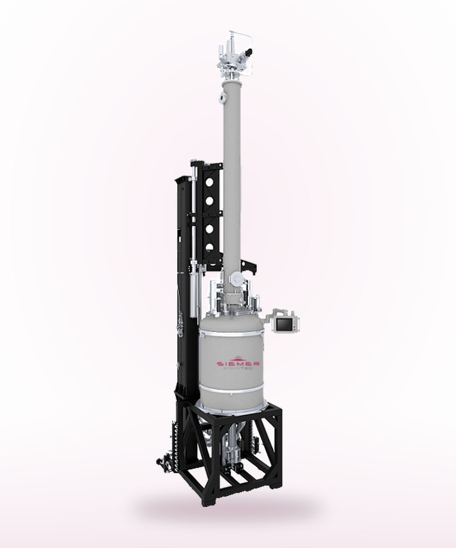
SIEMER ENERTEC low-oxygen monocrystalline crystal growth furnace
Crystal Growth

Low-oxygen monocrystalline crystal growth

Our crystal growth furnaces produce premium silicon ingots for next-generation photovoltaic applications. The proven Czochralski process runs inside a carefully controlled inert atmosphere, delivering high crystal quality, stable production and optimised oxygen concentration, the combination that modern n-type cell manufacturing demands.
  • Low oxygen crystal growth: thermal field engineering and optimised gas flow minimise oxygen incorporation, improving electrical characteristics
  • Fully automated pulling cycle: seeding, necking, shoulder, constant diameter and tail growth run without operator intervention
  • High-precision diameter control: closed-loop monitoring holds typical accuracy of ≤ ±0.5 mm, reducing material waste
  • Intelligent thermal management: optimised hot-zone design and control algorithms keep melt temperature stable across the full cycle
  • Modular architecture: configurable for different crystal sizes, with simplified maintenance and MES integration
  • Reduced operating cost: lower manual labour, material loss, energy consumption and downtime

More Information

Process Flow

Ingot section

Charge preparationPolysilicon charging, dopant addition, crucible loading and hot zone preparation.
Crystal growthSeeding, necking, crown, body and tail growth under automatic diameter control.
CroppingRemoval of seed and tail cones; ingot sectioning to workable lengths.
SquaringBand saw or diamond wire squaring to pseudo-square cross-section.
Grinding & chamferingSide grinding to final dimension, edge chamfering to reduce chipping.
Ingot qualificationResistivity, minority carrier lifetime, oxygen and carbon content, dislocation check.
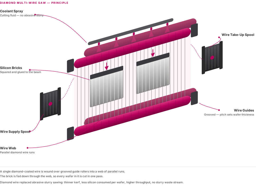
Diamond multi-wire saw principle: supply spool, wire web of parallel diamond wire runs over grooved guide rollers, silicon bricks fed down through the web under coolant spray, and take-up spool
Wafering

Diamond multi-wire sawing

Diamond wire cutting transformed the wafer stage. It enables thinner cuts, lower kerf loss and reduced silicon consumption while improving processing efficiency, wafer yield and surface quality, and it cuts wastewater and COD emissions substantially compared with the slurry processes it replaced.

Thin-wafer capability matters more with every generation. HJT and BC routes both benefit from thinner substrates, so we specify wire management, tension control and handling with headroom below current production thickness rather than at it.

  • 182 mm and 210 mm formats, rectangular variants on request
  • Thin wafer handling engineered for sub-130 μm processing
  • Wire consumption management as a designed cost parameter
  • Breakage-aware handling throughout transfer and cassette loading
Process Flow

Wafer section

Gluing & mountingIngot bonding to the beam for stable presentation to the wire web.
Diamond wire sawingMulti-wire cutting with tension and wire-speed control; kerf loss minimised.
De-bonding & degummingSeparation from the beam and removal of adhesive residues.
Pre-cleaning & rinsingRemoval of cutting debris and metallic contamination.
Cleaning & dryingChemical cleaning sequence and controlled drying without watermarks.
Inspection & sortingThickness, TTV, resistivity, geometry, photoluminescence microcrack detection, binning.

Why cleanliness is specified here, not later

HJT is exceptionally sensitive to metallic contamination and surface condition, because the thin intrinsic amorphous silicon passivation layer deposited later cannot compensate for a compromised surface. If HJT is your route, or a possible future route, the wafer cleaning and handling specification has to reflect that from the outset.

Output Specification

Typical line output parameters

Indicative figures for line sizing discussions. Final specification is set during the engineering phase against your product definition and site conditions.

Indicative parameters for capacity planning, not a product datasheet.
ParameterTypical specification
Material typen-type monocrystalline silicon (p-type available)
Wafer format182 mm and 210 mm; rectangular formats on request
Wafer thicknessConfigurable; thin-wafer capable for HJT and BC routes
Growth processCzochralski, RCZ and CCZ configurations
Wafering processDiamond multi-wire sawing
InspectionThickness, TTV, resistivity, geometry, PL microcrack detection
Automation interfaceCassette handling, AGV-ready load ports, MES data capture
Next Stage

Wafers feed the cell line

We will be happy to advise you

Tell us your target capacity, technology route and site conditions, and our engineering team will respond with a concrete line configuration.

Contact Us Now